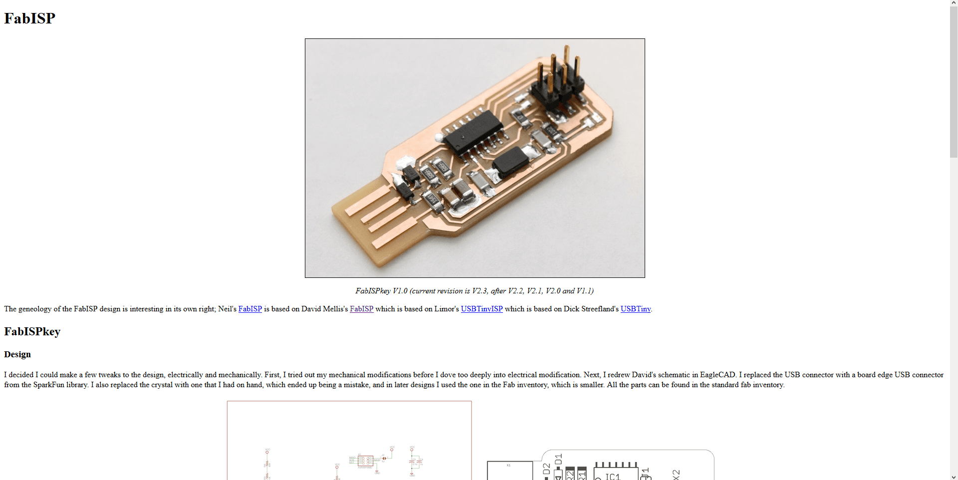
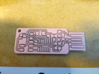
For electronics production I desided it would be fun to make a Fab ISP that could go on a keychain. This has been done before and I found I design online to use to create my first iteration. I downloaded the PNGs for the traces and outline. |

The traces I downloaded looked good, but one thing was missing that I will create myself and add a download link. That is, a stencil for applying solder paste before using a reflow station. |
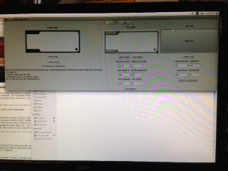
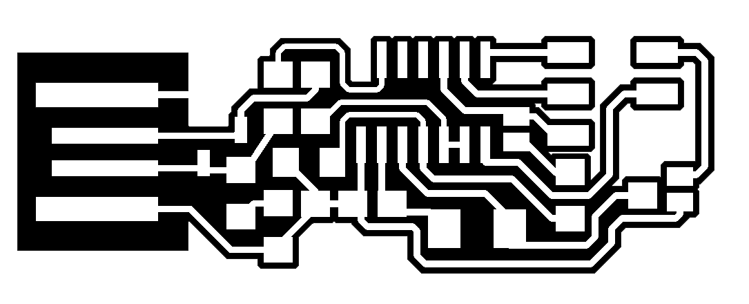
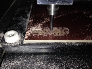
Using the Fab modules I opened the downloaded files for the Fab ISP(traces and outline). |
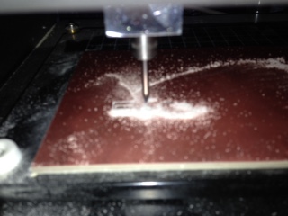
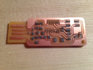
The mini mill is straightfoward. I set the z-axis to the height of my copper board and hit send. I cut the traces with a 1/64 bit and the default Fab module settings and the outline with a 1/32 bit. After the board was complete I noticed one thing. Near the usb port end of the Fab ISP there was excess copper. This I found out after tweeking some settings was an issue with the offset value. I found that for the Fab ISP a number between 4 and 6 works best. |
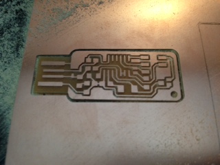
After the settings were adjusted and I cut out the Fab ISP again, it turned out great. |

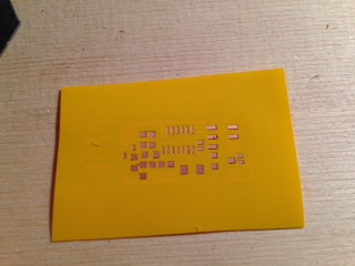
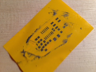
Back to what I was talking about in the beginning of this section, there is one thing that I thought was missing. I decided to make a stencil for the Fab ISP to help apply solder paste. I opened the PNG of the traces in Gimp and removed everything but the pads components will contact.Click here for my solder paste stencil file. |
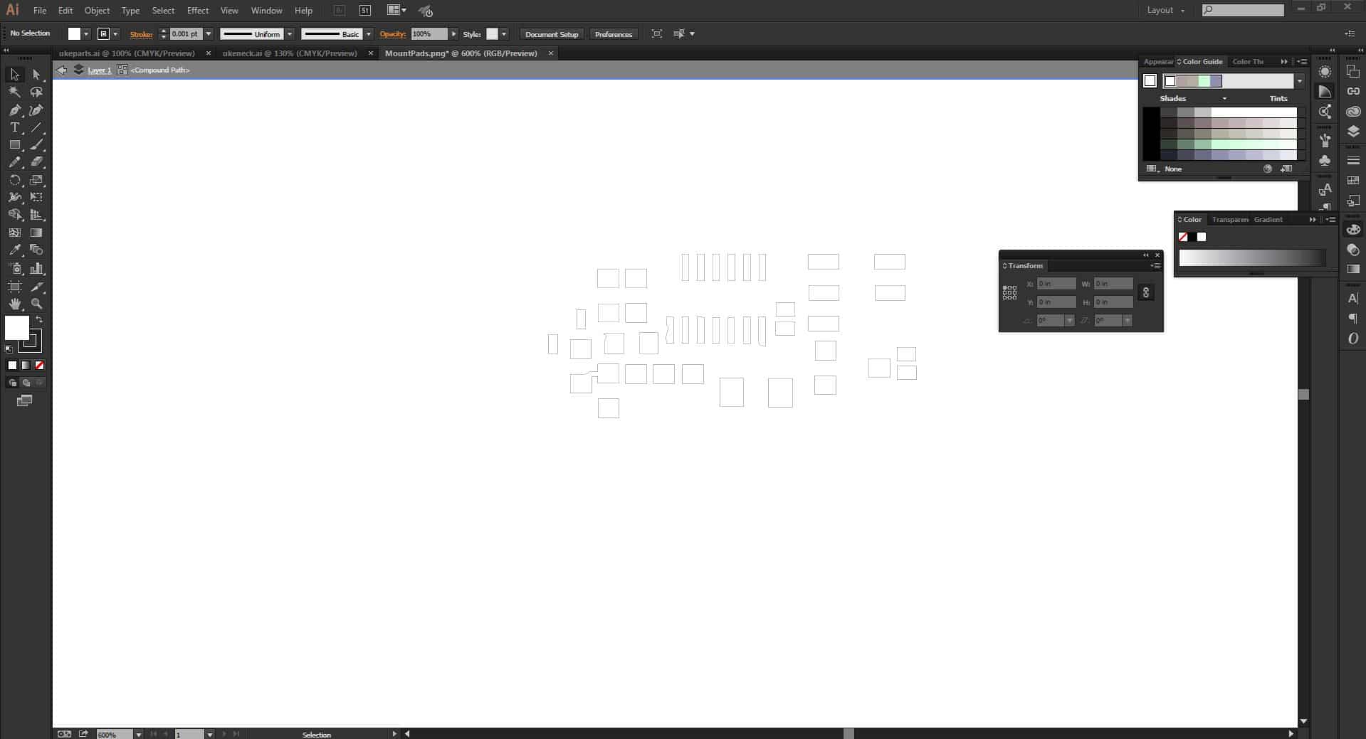
I then opened the file in Adobe Illustrator and traced the image to get a vector outline. From there I made sure to change the stroke to 0.001pt and clicked print to send it to the vinyl cutter. |
The first stencil I cut was alittle to messing. This was because I had the vinyl cutter set to the default cut speed. I found that turning down the vinyl cutter cut speed to the lowest setting in Adobe Illustrator helps give you a clean stencil. |
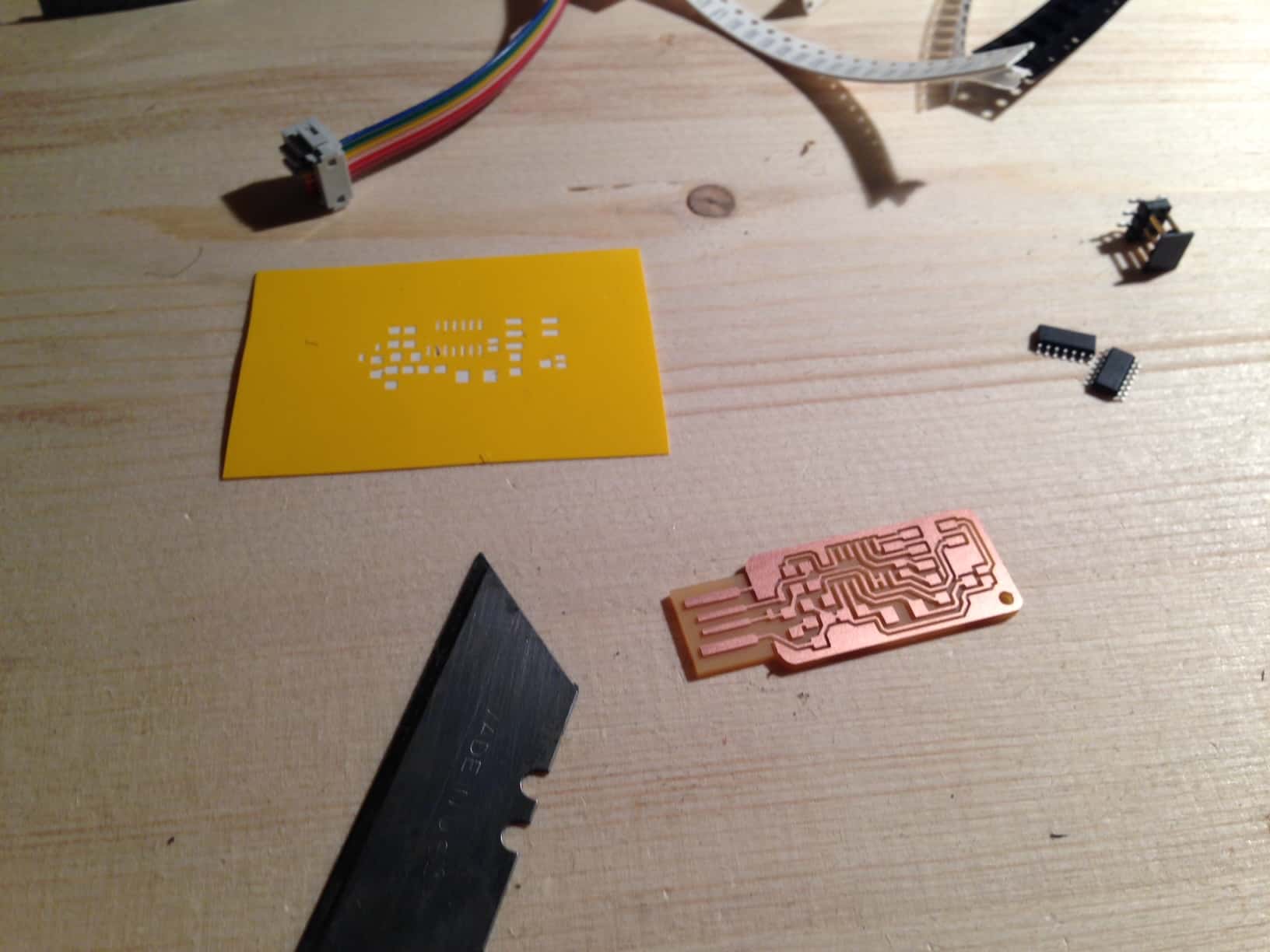
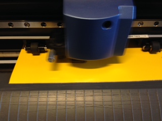
After getting the stencil and board cut out I was ready for assembly. A razor blade is a very handy tool for the next few steps, so make sure to find one. |
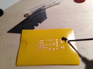
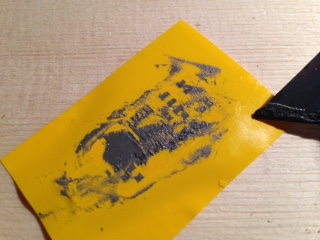
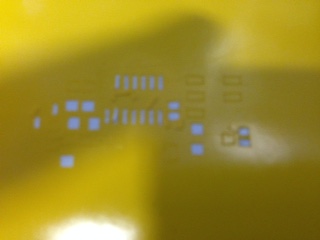
Next I put the vinyl stencil onto the circuit board being careful to line it up as accurately as possible. Then I added a dab of solder paste to the corner of the stencil and spread the paste around with the X-Acto blade. It may not seem like it but a tiny layer, just the thickness of the vinyl, it enough solder to connect your components. Leaving blobs of solder paste will often result in solder bridges and short circuits later in the process. |
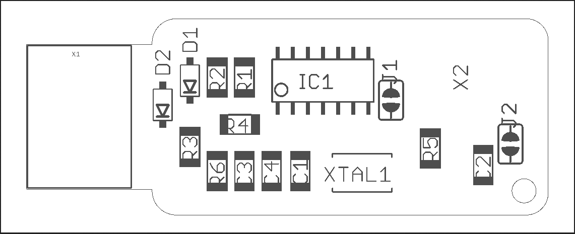
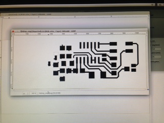
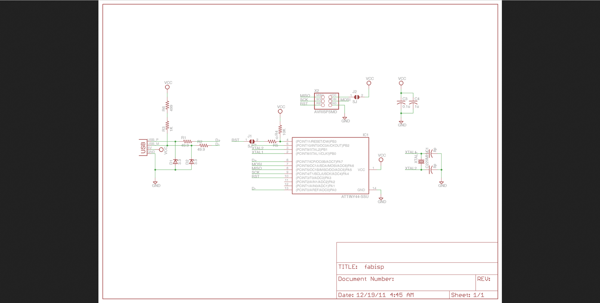
Once I wiped the excess solder paste off of the stencil I peeled it away. Then using ESD steezers(recommended but not totally necessary, regular tweezers work fine) I placed all of the components in their allocated positions on the board. The part numbers on the board layout shown above correspond to this Eagle schematic I downloaded. One thing you will notice when placing your components is that the components that connect to ground(most of the seemingly unused area with no traces in it) do not yet have solder on the side connected to ground because the stencil does not include these locations. Simply place the components and after soldering the sides connecting to the traces, using a re-flow station or soldering iron if you are feeling confindent, place a dab of solder on the ground side and solder the grounds. Just a Note: I would recomend using a hot air reflow station such as the one solder by Sparkfun, I use a temp of ~270 celsius and an airflow of ~2 so that I do not blow the components out of place. |
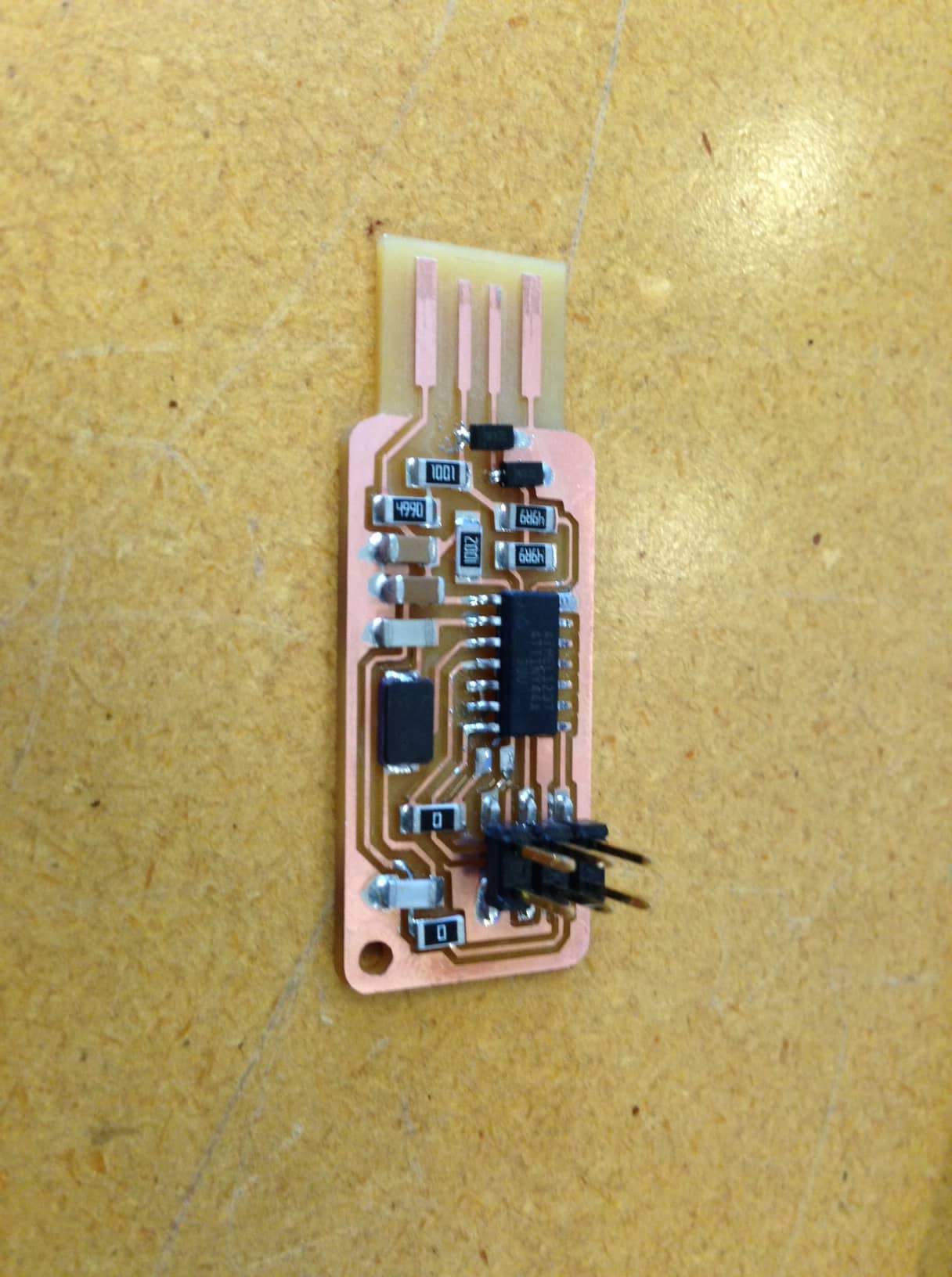
Don't worry the fun is not over yet. Once all of the components are on and both jumpers are in place(you can make a solder bridge or use a 0 ohm resistor) you are ready to program your new FAB ISP. |
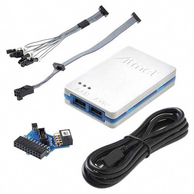
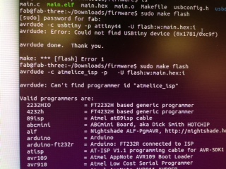
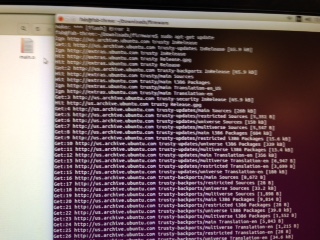
To program my FAB ISP I used Ubuntu, I prefer Linux Mint but Ubuntu works well and that's what we had on the computers in the lab. If you are using a new programmer like the Atmel ICE(which I highly recommend- its available in barebones for $38 or complete kit for $100) avrdude will probably not recognize your device. That meant I had to update AVRDUDE, so in terminal I typed "sudo apt-get update". After the update simply restart your computer to apply the updates and AVRDUDE should recognize the new device, if not simply download the newest version of AVRDUDE using terminal commands. |
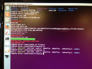
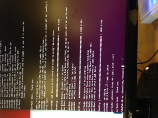
Once AVRDUDE is updated plug your programmer into your computer and connect your FAB ISP to the programmer and a USB port on the computer. Then if you have not already download a Fab ISP make files. This can be done easily with the "wget http://academy.cba.mit.edu/classes/embedded_programming/firmware.zip" command in terminal. Once this is downloaded navigate to the folder in which you just downloaded the files using terminal and unzip the zip file. From there open the make file and change the programmer to your programmer. In my case I was using an Atmel ICE programmer. Note: The Atmel ICE is a programmer and debugger so you must use the name "atmelice_isp" to use it for programming AVR microcontrollers. Finally once you are in the folder containing the make file use these commands. 1. "make clean" 2. "make hex" 3. "sudo make fuse" (if you have not already used a sudo command in your terminal session then it will prompt you for your password if you have one0 4. "sudo make program". If all of the commands work well you are done. I used the command lsusb to check for usb devices afterwords and if everything worked you should be able to see your FAB ISP which will be named something like "Multiple Vendors USBTiny". Finally I unsoldered the solder jumper 1 which is labeled "J1" in the schematic and my ISP was done. |
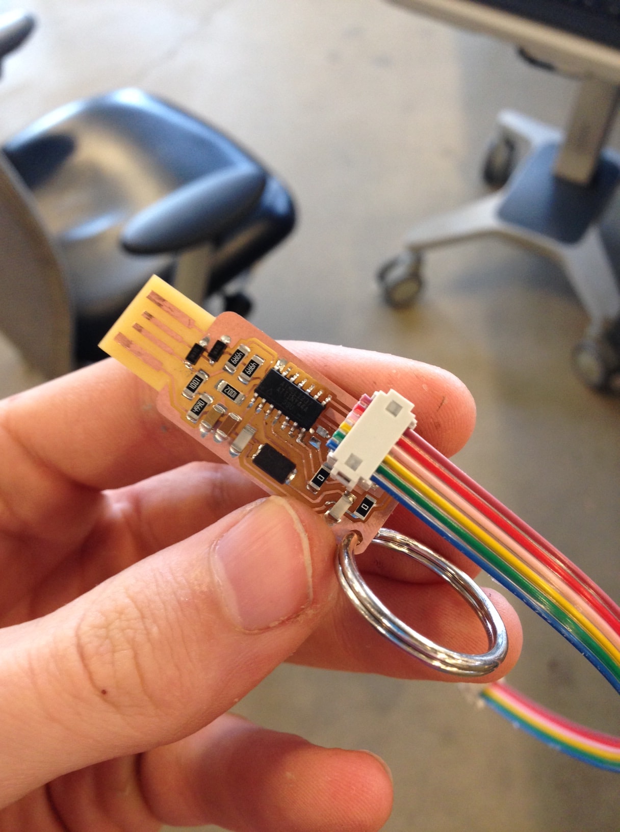
To finish it all of I added a 6 pin ribbon cable I made using a clamp and some cable and plugs to communicate with microprocessors and a key ring to the hole in the side so I could attack it to my wallet or keychain. It is also a good idea to add some tap to the bottom of the USB section and a layer of solder to the top of the USB contacts to ensure good contact with USB ports. |